
The controllable preparation of high-quality graphene is the basis of various basic researches and application developments, and it is one of the major basic scientific issues that urgently requires in-depth study. This area of ​​research involves the control of its size, morphology, boundaries, the degree of crystal structure perfection, doping, etc., in order to achieve its electrical performance control.
With the strong support of the Chinese Academy of Sciences, the Ministry of Science and Technology, and the National Natural Science Foundation of China, in response to these scientific problems, the related researchers of the organic solids laboratory of the Institute of Chemistry, Chinese Academy of Sciences, have been working on the basis of controllable preparation of graphene and Significant progress has been made in performance research. The results were published in Adv. Mater., NPG Asia Mater., J. Am. Chem. Soc. and Nat. Commun.
Graphene is grown directly on the dielectric layer. Chemical vapor deposition (CVD) has become one of the most important methods for the preparation of graphene because it combines the advantages of high quality and macro quantities. However, graphene prepared by this method generally needs to be transferred to other dielectric layers to prepare graphene devices and circuits. The transfer process will cause problems such as graphene damage, wrinkles, contamination, and material waste. Therefore, whether the graphene can be directly grown on the dielectric layer has important scientific significance and huge technical requirements. Graphene is grown directly on the dielectric layer and is compatible with current silicon electronics processing techniques and can be used directly for device fabrication and assembly.
In the previous work, researchers at the Institute of Organic Solids Laboratory invented the oxygen-assisted method to directly prepare graphene films on silicon dioxide insulation materials (J. Am. Chem. Soc. 2011, 133, 17548). It was found that the nucleation sites and crystallite size of graphene can be controlled by two chemical vapor deposition methods, and the high-quality graphene film can be directly grown on the surface of silicon nitride.
The size of the graphene domain crystals in the prepared graphene film was 1 μm. The film has high electrical properties and its mobility can reach 1510 cm2V-1s-1 in air and 1518 cm2V-1s-1 in nitrogen. These properties have been doubled compared to graphene films grown directly on silica substrates and have been higher than that of some metal-catalyzed graphenes. The research results were published in Advanced Materials (Adv. Mater., 2013, 25, 992) and were selected as the inside cover.
Morphology regulation and etching of single crystal graphene. The preparation of monocrystalline graphene and the regulation of its boundary structure are the frontier topics widely recognized in the study of controlled preparation of graphene. The latter goal is particularly confronted with the dual challenges of lack of theoretical guidance and concrete solutions. Researchers at the Chemtronics Solid State Laboratory used the isotropic CVD method of liquid copper surface to prepare regular hexagonal monocrystalline graphene (Proc. Natl. Acad. Sci. USA, 2012, 109, 7992). A series of new thermodynamic graphene metastable structures were obtained for the first time through the regulation of the microscopic kinetics of graphene nucleation and growth (continuous control of the ratio of Ar and H2).
The morphology of this series of graphenes with a high degree of sixfold symmetry follows a definite pattern of change: the graphene boundary variation encompasses a complete range of changes from positive curvature to negative curvature. This graphene pattern system is strikingly similar to the snowflake structure collection in nature, and represents the only example of a known material that perfectly reproduces a snowflake structure set in a two-dimensional manner that is simpler (snowflake is a three-dimensional crystal).
Based on the above facts, the universal growth mechanism of diffusion control is further proposed and is consistent with the theoretical simulation. This work has for the first time linked the growth and morphology regulation of graphene with the kinetic regulation of non-equilibrium systems, revealing a never-found but universally-existing basic rule of graphene growth, which can be generalized to A more extensive two-dimensional atomic crystal material. The related work was published in the "Nature Materials" (NPG Asia Mater., 2013, 5, e36) of the Nature Press Group.
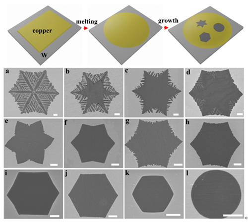
Perfect regulation of the morphology/boundary of monocrystalline graphene
Based on this work, researchers applied this regulation method to the study of graphene etching behavior. The traditional experimental results and concepts suggest that due to the regular arrangement of the building elements, the etching of the perfect crystal behaves as anisotropic etching, and the etching pattern is characterized by a simple Euclidean geometry. The previous experimental results also show that the graphene follows This rule.
The researchers adjusted the ratio of the etching gas H2 to the inert gas Ar, revealing for the first time that the etching pattern of graphene can greatly deviate from the ideal anisotropic etching mode, making the graphene etching pattern from the simple Euclidean From the evolution of structurally complex fractal structures (Figure 3), the simple Euclid etching patterns of graphene observed in previous studies are only special cases of this general evolutionary process. Related work was published in the "J. Am. Chem. Soc. 2013, 135, 6431". The "Chemistry World" of the Royal Society of Chemistry reported the results on the headline of its home page under the heading "Carving graphene snowflakes with gases". "These beautiful snowflakes are not composed of ice but etched from graphene sheets. to".

Graphene fractal etch pattern
Single-walled carbon nanotubes / graphene with intramolecular junctions. Dr. Wei Dacheng of the National University of Singapore and Professor ATSWee collaborated with relevant staff of the organic solids laboratory to prepare single-walled carbon nanotube/graphene ribbon intramolecular junctions (Figure 4). The intramolecular junction shows typical asymmetrical rectification curves ( Switching ratio: ~160,at ±1.5 V). The photocurrent and photovoltage are linearly and exponentially related to the laser intensity. At a light intensity of 98.6 kW/cm2, high photocurrent (11.6 nA) and high light are obtained respectively. The voltage (270 mV) and external photosensitivity of 3 mA/W are higher than those of the two-dimensional graphene or carbon nanotube pn junction, indicating that the intramolecular junction energy is expected to be a high-performance photodetector. The results were published on Nat. Commun. (2013, 4, 1374).
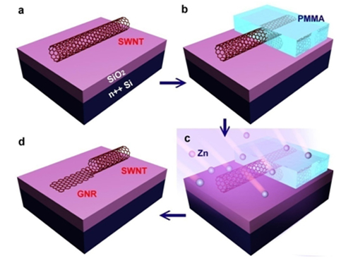
Preparation of single-walled carbon nanotube/graphene ribbon intramolecular junction
This series of work reveals the rich content of graphene growth process under non-equilibrium conditions, providing a broad research space for its further controllable preparation of high-quality, large-area, non-polluting graphene. The results of these studies are also a general reference for the understanding of material growth processes in non-equilibrium systems, and also some basic physical concepts and natural phenomena in graphene and science (such as disorder and order, certainty and randomness, and simplicity To complex, liquid, snow, etc.) are closely linked.
Product name:Torsion Spring Steel Wire
Standards:
DIN 17223-1 Round Steel Wire For Springs
DIN EN 10270-1 Steel Wire For Mechanical Springs
GB 3206-82 Carbon Constructional Quality Steel Wire
JIS G 3521-1991 Hard Drawn Steel Wire
GB 4357-89 Carbon Spring Steel Wire
YB/T 5220-93 Carbon Steel Wire For Non-Mechanical Springs
Diameter: 0.20mm-12.50mm
Usages: torsion spring,wire forming springs.
Material: 30MnSi, 62A,62B, 60, 65, 65Mn, 70, 75,72A, 72B, 77A, 77B, 80,82A, 82B
Torsion Spring Steel Wire
Torsion Spring Steel Wire,Torsion Car Spring Wire,Car Spring Wire,Torsion Spring Wire
TAIXING HONGYE STEEL WIRE MANUFACTURING CO.,LTD , http://www.steeltr.com